Creating ultrasmall grooves on microchips — a key part of many modern technologies — is about to become as easy as making a sandwich, using a new process invented by Princeton engineers.
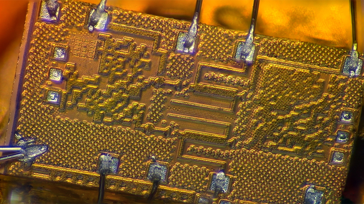
The simple, low-cost technique results in the self-formation of periodic lines, or gratings, separated by as few as 60 nanometers — less than one ten-thousandth of a millimeter — on microchips. Features of this size have many uses in optical, biological and electronic devices, including the alignment of liquid crystals in displays. The researchers will publish their findings Sept. 2 in the online version of Nature Nanotechnology.
“It’s like magic,” said electrical engineer Stephen Chou , the Joseph C. Elgin Professor of Engineering. “This is a fundamentally different way of making nanopatterns.”
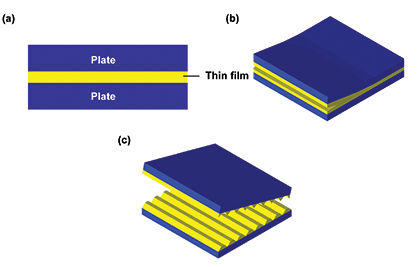
The process, called fracture-induced structuring, is as easy as one-two-three. First, a thin polymer film is painted onto a rigid plate, such as a silicon wafer. Then, a second plate is placed on top, creating a polymer sandwich that is heated to ensure adhesion. Finally, the two plates are pried apart. As the film fractures, it automatically breaks into two complementary sets of nanoscale gratings, one on each plate. The distance between the lines, called the period, is four times the film thickness.

The ease of creating these lines is in marked contrast to traditional fabrication methods, which typically use a beam of electrons, ions or a mechanical tip to “draw” the lines into a surface. These methods are serial processes which are extremely slow and therefore only suitable for areas one square millimeter or smaller. Other techniques suitable for larger areas have difficulties achieving small grating periods or producing a high yield, or they require complex and expensive processes. Fracture-induced structuring is not only simple and fast, but it enables patterning over a much larger area. The researchers have already demonstrated the ability of the technique to create gratings over several square centimeters, and the patterning of much large areas should be possible with further optimization of the technique.
“It’s remarkable — and counterintuitive — that fracturing creates these regular patterns,” said William Russel, dean of the Graduate School and the Arthur W. Marks ’19 Professor of Chemical Engineering. Russel and his graduate student Leonard Pease III teamed with Chou and his graduate students Paru Deshpande and Ying Wang to develop the technique.
A patent application has been filed on the process, which the researchers say is economically feasible for large-scale use in industry. The gratings generated by the fracturing process also could be used in conjunction with existing patterning methods. For example, the nanoimprinting method invented by Chou in the 1990s can use the gratings generated by fracture-induced structuring to create a mold that enables mass duplication of patterns with high precision at low cost.
As with many scientific discoveries, the fracture-induced structuring process was happened upon accidentally. Graduate students in the Chou and Russel groups were trying to use instabilities in various molten polymers (in essence, melted plastic) to create patterns when they discovered instead that fracturing a solid polymer film can generate the gratings automatically. The team seized upon this finding and established the optimal conditions for grating formation.
Next, the group plans to explore the fundamental science behind the process and investigate the interplays of various forces at such a small scale, according to Chou.
“And, we want to push the limit and see how small we can go,” he said.
The work was supported by a National Science Foundation Materials Research Science and Engineering Centers grant, the Defense Advanced Research Projects Agency, the Office of Naval Research and the Department of Defense.
Abstract:
Self-formation of sub-60-nm half-pitch gratings with large areas through fracturing
Periodic micro- and nanostructures (gratings) have many significant applications in electronic, optical, magnetic, chemical and biological devices and materials. Traditional methods for fabricating gratings by writing with electrons, ions or a mechanical tip are limited to very small areas and suffer from extremely low throughput. Interference lithography can achieve relatively large fabrication areas, but has a low yield for small-period gratings. Photolithography, nanoimprint lithography, soft lithography and lithographically induced self-construction all require a prefabricated mask, and although electrohydrodynamic instabilities can self-produce periodic dots without a mask, gratings remain challenging. Here, we report a new low-cost maskless method to self-generate nano- and microgratings from an initially featureless polymer thin film sandwiched between two flat relatively rigid plates. By simply prying apart the plates, the film fractures into two complementary sets of nonsymmetrical gratings, one on each plate, of the same period. The grating period is always four times the thickness of the glassy film, regardless of its molecular weight and chemical composition. Periods from 120 nm to 200 mm have been demonstrated across areas as large as two square centimeters.


