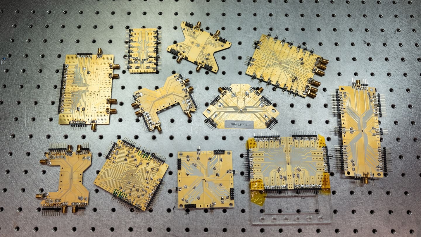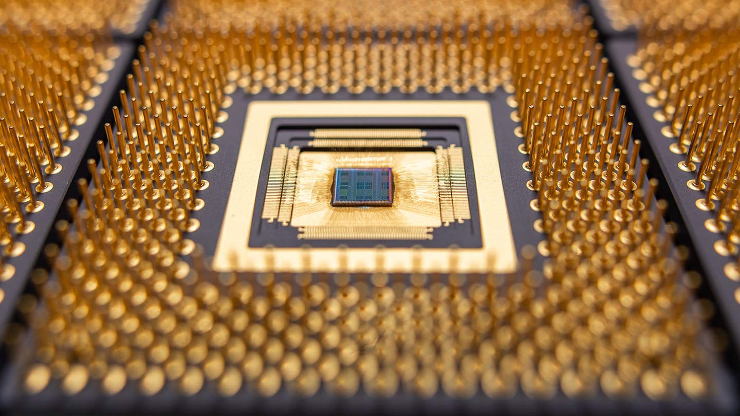
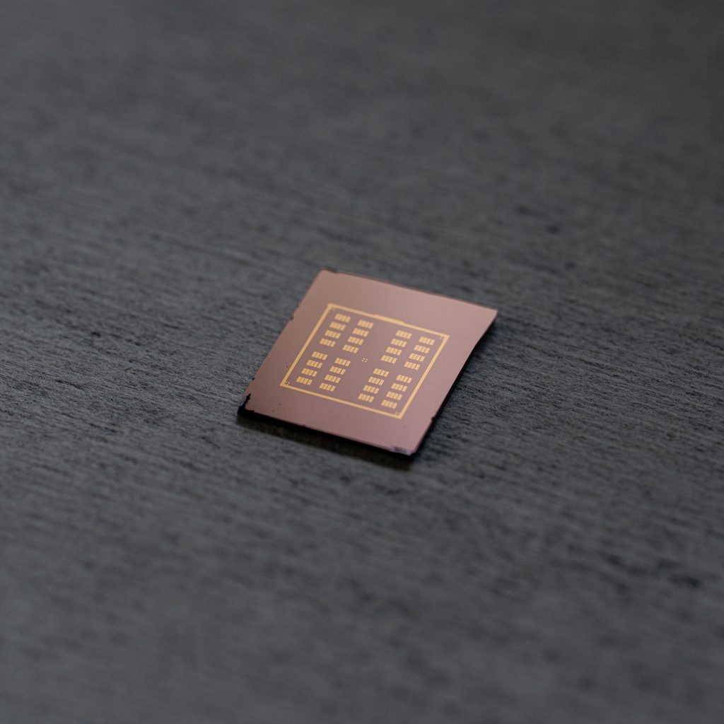
Researchers at Princeton engineering have created a semiconductor with unique properties: it is just a few molecules thick and can repeatedly change its properties in response to light. This is a step toward building more energy-efficient sensors, optoelectronic devices and computing technologies.
Advances in semiconductors over the last 50 years have allowed engineers to create increasingly smaller semiconductor devices and power more efficient computers. But this approach is reaching its physical limits — the semiconductor devices are so tiny it is challenging to add more. Researchers are now creating new materials rather than shrinking existing ones.
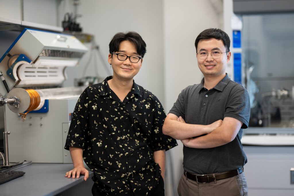
“One of the future goals for advancing electronics is not just making materials smaller, but making them adaptable and smarter,” said Jaehoon Ji, post-doctoral researcher and first author on the July 1 paper describing the research in Science Advances.
Current semiconductors, used to power everything from televisions to laptops to microwaves, respond to electrical signals. Once manufactured, the way they conduct electricity remains largely unchanged. This new material, by contrast, is responsive and changeable.
“The first step to creating smart materials is responsiveness,” said Saien Xie, assistant professor of electrical and computer engineering and the paper’s lead author. “Living systems are extremely smart, because they continuously sense and respond to their surroundings. We wanted to create a material that can similarly respond to external stimuli instead of remaining permanently fixed.”
To accomplish that goal, the team combined a super thin semiconductor with light-responsive molecules that change structure when exposed to different wavelengths. These changes alter the semiconductor’s electronic properties, allowing its conductivity and optical response to be programmed, erased, and reprogrammed with light.
This means that the material does not function like a simple on-off switch. “Instead of switching directly from zero to one, we can gradually adjust the material’s response and then reverse the process,” Ji said.
Xie, Ji and their collaborators have created a uniform piece of this super thin semiconductor that is one inch square. Using this, they have built arrays of programmable electronic switches, a step toward larger integrated systems. Next, they are working to connect these switches into a circuit, a fundamental building block for any complex electronic device.
“Our long-term vision is to build electronics whose functionality is no longer fixed during fabrication,” Xie said. “Instead, we want devices whose properties can be dynamically reconfigured after they are made. This work demonstrates an important step toward that goal.”
The paper, Large-area, photo-programmable 2D semiconductors with chromic molecular functionalization, was published July 1 in Science Advances. In addition to Xie and Ji, authors include Yin Liang, Jinpeng Tian, Jingtao Tan, Jaerin Kim, Satya Butler, Haining Mao and Gloria Liu at Princeton University. The research was primarily supported by the Eric and Wendy Schmidt Transformative Technology Fund, David and Lucile Packard Foundation and the National Science Foundation Materials Research Science and Engineering Center under grant number DMR-2011750.