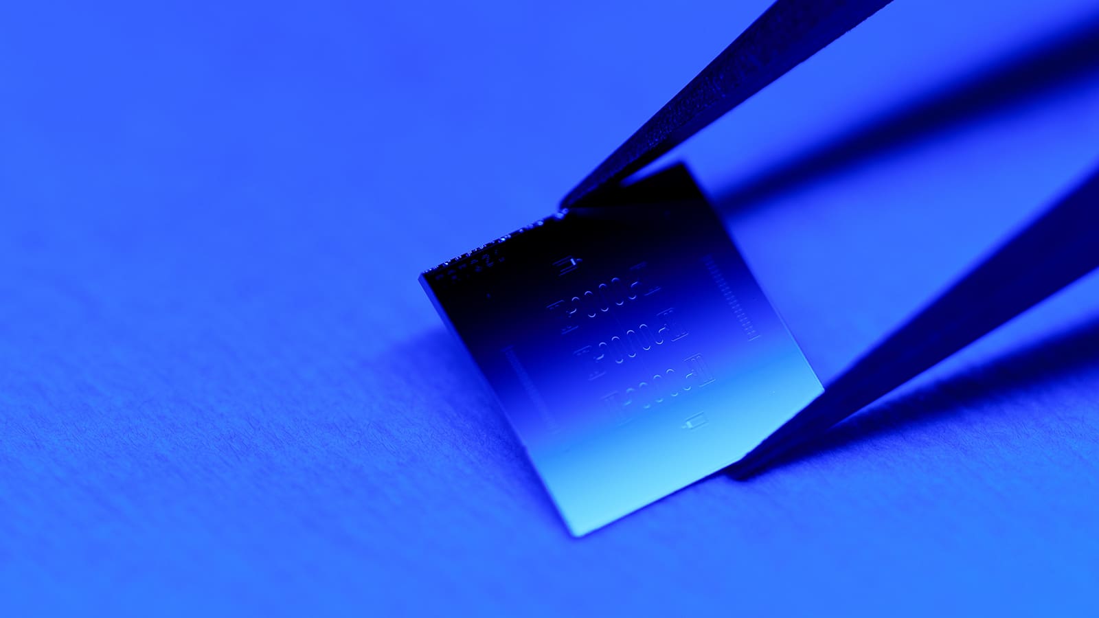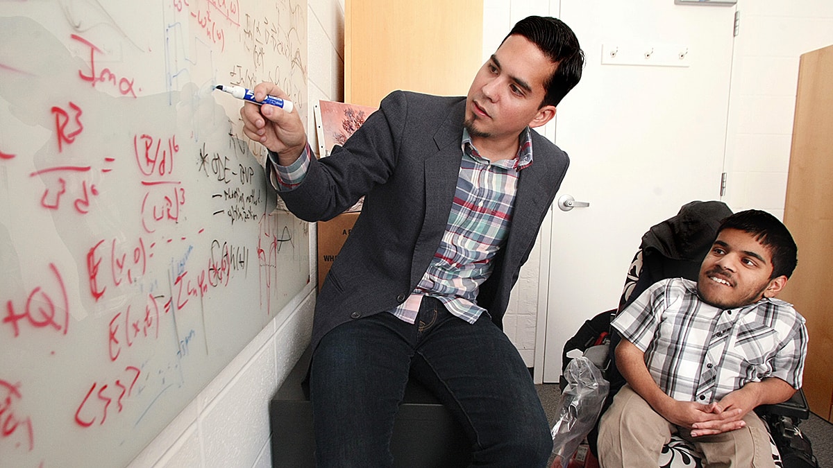
The new hardware reimagines AI chips for modern workloads and can run powerful AI systems using much less energy than today’s most advanced semiconductors, according to Naveen Verma, professor of electrical and computer engineering. Verma, who will lead the project, said the advances break through key barriers that have stymied chips for AI, including size, efficiency and scalability.
Chips that require less energy can be deployed to run AI in more dynamic environments, from laptops and phones to hospitals and highways to low-Earth orbit and beyond. The kinds of chips that power today’s most advanced models are too bulky and inefficient to run on small devices, and are primarily constrained to server racks and large data centers.
Now, the Defense Advanced Research Projects Agency, or DARPA, has announced it will support Verma’s work, based on a suite of key inventions from his lab, with an $18.6 million grant. The DARPA funding will drive an exploration into how fast, compact and power-efficient the new chip can get.
“There’s a pretty important limitation with the best AI available just being in the data center,” Verma said. “You unlock it from that and the ways in which we can get value from AI, I think, explode.”
The announcement came as part of a broader effort by DARPA to fund “revolutionary advances in science, devices and systems” for the next generation of AI computing. The program, called OPTIMA, includes projects across multiple universities and companies. The program’s call for proposals estimated total funding at $78 million, although DARPA has not disclosed the full list of institutions or the total amount of funding the program has awarded to date.
In the Princeton-led project, researchers will collaborate with Verma’s startup, EnCharge AI. Based in Santa Clara, Calif., EnCharge AI is commercializing technologies based on discoveries from Verma’s lab, including several key papers he co-wrote with electrical engineering graduate students going back as far as 2016.
Encharge AI “brings leadership in the development and execution of robust and scalable mixed-signal computing architectures,” according to the project proposal. Verma co-founded the company in 2022 with Kailash Gopalakrishnan, a former IBM Fellow, and Echere Iroaga, a leader in semiconductor systems design.
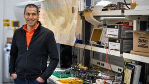
Gopalakrishnan said that innovation within existing computing architectures, as well as improvements in silicon technology, began slowing at exactly the time when AI began creating massive new demands for computation power and efficiency. Not even the best graphics processing unit (GPU), used to run today’s AI systems, can mitigate the bottlenecks in memory and computing energy facing the industry.
“While GPUs are the best available tool today,” he said, “we concluded that a new type of chip will be needed to unlock the potential of AI.”
The needs are real
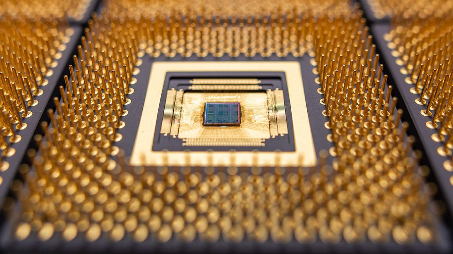
Between 2012 and 2022, the amount of computing power required by AI models grew by about 1 million percent, according to Verma, who is also director of the Keller Center for Innovation in Engineering Education at Princeton University. To meet demand, the latest chips pack in tens of billions of transistors, each separated by the width of a small virus. And yet the chips still are not dense enough in their computing power for modern needs.
Today’s leading models, which combine large language models with computer vision and other approaches to machine learning, were developed using more than a trillion variables each. The Nvidia-designed GPUs that have fueled the AI boom have become so valuable, major companies reportedly transport them via armored car. The backlogs to buy or lease these chips stretch to the vanishing point.
When Nvidia became only the third company ever to reach a $2 trillion valuation, the Wall Street Journal reported that a rapidly increasing share of the company’s rising revenue came not through the development of the models, called training, but in chips that enable the use of AI systems once they are already trained. Technologists refer to this deployment stage as inference. And inference is where Verma says his research will have the most impact in the near-to-medium term.
“This is all about decentralizing AI, unleashing it from the data center,” he said. “It’s got to move out of the data center into places where we and the processes that matter to us can access computing the most, and that’s phones, laptops, factories, those kinds of things.”
Freeing AI from the cloud
To create chips that can handle modern AI workloads in compact or energy-constrained environments, the researchers had to completely reimagine the physics of computing while designing and packaging hardware that can be manufactured with existing fabrication techniques and that can work well with existing computing technologies, such as a central processing unit.
“AI models have exploded in their size,” Verma said, “and that means two things.” AI chips need to become much more efficient at doing math and much more efficient at managing and moving data.
Their approach has three key parts.
The core architecture of virtually every digital computer has followed a deceptively simple pattern first developed in the 1940s: store data in one place, do computation in another. That means shuttling information between memory cells and the processor. Over the past decade, Verma has pioneered research into an updated approach where the computation is done directly in memory cells, called in-memory computing. That’s part one. The promise is that in-memory computing will reduce the time and energy it costs to move and process large amounts of data.
But so far, digital approaches to in-memory computing have been highly limited. Verma and his team turned to an alternate approach: analog computation. That’s part two.
“In the special case of in-memory computing, you not only need to do compute efficiently,” Verma said, “you also need to do it with very high density because now it needs to fit inside these very tiny memory cells.” Rather than encoding information in a series of 0s and 1s, and processing that information using traditional logic circuits, analog computers leverage the richer physics of the devices. The curvature of a gear. The ability of a wire to hold electrical charge.
Digital signals began replacing analog signals in the 1940s primarily because binary code scaled better with the exponential growth of computing. But digital signals don’t tap deeply into the physics of devices, and as a result they can require more data storage and management. They are less efficient in that way. Analog gets its efficiency from processing finer signals using the intrinsic physics of the devices. But that can come with a tradeoff in precision.
“The key is in finding the right physics for the job in a device that can be controlled exceedingly well and manufactured at scale,” Verma said.
His team found a way to do highly accurate computation using the analog signal generated by capacitors specially designed to switch on and off with exacting precision. That’s part three. Unlike semiconductor devices such as transistors, the electrical energy moving through capacitors doesn’t depend on variable conditions like temperature and electron mobility in a material.
“They only depend on geometry,” Verma said. “They depend on the space between one metal wire and the other metal wire.” And geometry is one thing that today’s most advanced semiconductor manufacturing techniques can control extremely well.