src=”/wp-content/uploads/chou_ramansensor_inside.jpg” title=”Micrograph of a sensor
developed at Princeton for sensing Raman scattering. Pillars support metal components that gather light and
amplify Raman signals, wavelengths of light that can be used to identify a substance. (Credit: Stephen Y.
Chou)” width=”500″ />
Princeton researchers have invented an extremely sensitive sensor that opens up new ways to detect
a wide range of substances, from tell-tale signs of cancer to hidden explosives.
The sensor, which is the most sensitive of its kind to date, relies on a completely new
architecture and fabrication technique developed by the Princeton researchers.
The device boosts faint signals generated by the scattering of laser light from a material placed
on it, allowing the identification of various substances based on the color of light they reflect. The
sample could be as small as a single molecule.
The technology is a major advance in a decades-long search to identify materials using Raman
scattering, a phenomenon discovered in the 1920s by an Indian physicist, Chandrasekhara Raman, where light
reflecting off an object carries a signature of its molecular composition and structure.
“Raman scattering has enormous potential in biological and chemical sensing, and could
have many applications in industry, medicine, the military and other fields,” said Stephen”>https://www.princeton.edu/ee/people/display_person/?netid=chou”>Stephen
Chou, the professor of electrical”>http://www.princeton.edu/ee/”>electrical
engineering who led the research team. “But current Raman sensors are so weak that their
use has been very limited outside of research. We’ve developed a way to significantly enhance the
signal over the entire sensor and that could change the landscape of how Raman scattering can be used.”
Chou and his collaborators, electrical engineering graduate students, Wen-Di Li and Fei Ding, and
post-doctoral fellow, Jonathan Hu, published a paper on their innovation in February in the journal
href=”Optics”>http://www.opticsinfobase.org/oe/abstract.cfm?URI=oe-19-5-3925″>Optics Express.
The research was funded by the Defense”>http://ttp://www.darpa.mil/”>Defense Advance
Research Projects Agency.
In Raman scattering, a beam of pure one-color light is focused on a target, but the reflected light
from the object contains two extra colors of light. The frequency of these extra colors are unique to the
molecular make-up of the substance, providing a potentially powerful method to determine the identity of the
substance, analogous to the way a finger print or DNA signature helps identify a person.
Since Raman first discovered the phenomenon – a breakthrough that earned him Nobel Prize
– engineers have dreamed of using it in everyday devices to identify the molecular composition and
structures of substances, but for many materials the strength of the extra colors of reflected light was too
weak to be seen even with the most sophisticated laboratory equipment.
Researchers discovered in the 1970s that the Raman signals were much stronger if the substance to
be identified is placed on a rough metal surface or tiny particles of gold or silver.
The technique, known as surface enhanced Raman scattering (SERS), showed great promise, but even
after four decades of research has proven difficult to put to practical use. The strong signals appeared
only at a few random points on the sensor surface, making it difficult to predict where to measure the
signal and resulting in a weak overall signal for such a sensor.
Abandoning the previous methods for designing and manufacturing the sensors, Chou and his
colleagues developed a completely new SERS architecture: a chip studded with uniform rows of tiny pillars
made of metals and insulators.

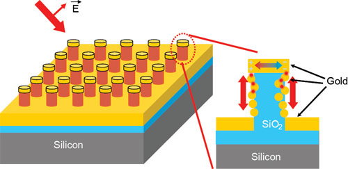
title=”Schematic showing the architecture of the sensor developed at Princeton.” width=”500″
/>
One secret of the Chou team’s design is that their pillar arrays are fundamentally
different from those explored by other researchers.
Their structure has two key components: a cavity formed by metal on the top and at the base of each
pillar; and metal particles of about 20 nanometers in diameter, known as plasmonic nanodots, on the pillar
wall, with small gaps of about 2 nanometers between the metal components.
The small particles and gaps significantly boost the Raman signal. The cavities serve as antennae,
trapping light from the laser so it passes the plasmonic nanodots multiple times to generate the Raman
signal rather than only once. The cavities also enhance the outgoing Raman signal.
The Chou’s team named their new sensor “disk-coupled dots-on-pillar
antenna-array” or D2PA, for short.
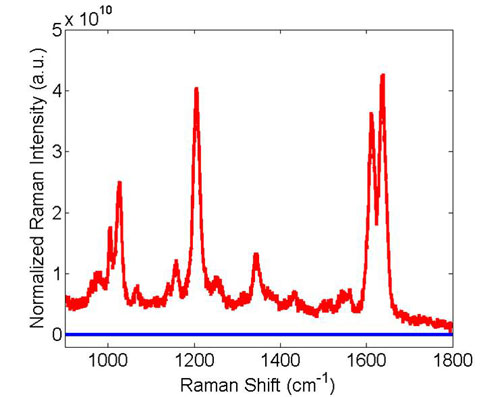
So far, the chip is a billion times more sensitive than was possible without SERS boosting of Raman
signals and the sensor is uniformly sensitive, making it more reliable for use in sensing devices. Such
sensitivity is several orders of magnitude higher than the previously reported.

title=”This graph shows Raman signal boosted by the Princeton sensor (red) compared to an unenhanced
signal (blue).” width=”500″ />
Already, researchers at the U.S. Naval Research Laboratory are experimenting with a less sensitive
chip to explore whether the military could use the technology pioneered at Princeton for detecting
chemicals, biological agents and explosives.
In addition to being far more sensitive than its predecessors, the Princeton chip can be
manufactured inexpensively at large sizes and in large quantities. This is due to the easy-to-build nature
of the sensor and a new combination of two powerful nanofabrication technologies: nanoimprint, a method that
allows tiny structures to be produced in cookie-cutter fashion; and self-assembly, a technique where tiny
particles form on their own.
Chou’s team has produced these sensors on 4-inch wafers (the basis of electronic chips) and
can scale the fabrication to much larger wafer size.
“This is a very powerful method to identify molecules,” Chou said. “The
combination of a sensor that enhances signals far beyond what was previously possible, that’s
uniform in its sensitivity and that’s easy to mass produce could change the landscape of sensor
technology and what’s possible with sensing.”
Citation:
Wen-Di Li, Fei Ding, Jonathan Hu, and Stephen Y. Chou, “Three-dimensional cavity nanoantenna
coupled plasmonic nanodots for ultrahigh and uniform surface-enhanced Raman scattering over large area,”
Opt. Express 19, 3925-3936 (2011) URL: http://www.opticsinfobase.org/oe/abstract.cfm?URI=oe-19-5-3925
“>http://www.opticsinfobase.org/oe/abstract.cfm?URI=oe-19-5-3925“>http://w…


