Princeton engineers have invented an affordable technique that uses lasers and plastic beads to create the ultrasmall features that are needed for new generations of microchips.
The method, which creates lines and dots that are 1,000 times narrower than a human hair, may enable the creation of biological computers as well as micromachines with applications in medicine, optical communications, computing and sensor technologies.
The technique, created by mechanical and aerospace engineering assistant professor Craig Arnold and graduate student Euan McLeod, is similar to poising a magnifying lens over a scrap of paper and angling the lens to focus sunlight and ignite the paper. In place of the lens, the researchers use a microscopic plastic bead floating in water to focus light from a powerful laser and burn designs onto a blank microchip. Their findings are reported online June 8 in the journal Nature Nanotechnology.

While others have passed laser light through various microscopic objects to pattern surfaces, they have struggled to maintain a consistent distance between the bead and the surface of the microchip. If this distance changes, the laser light is focused in different ways across the surface and the resulting pattern is inconsistent. Arnold and McLeod established an innovative way to ensure that the bead is always the same distance from the microchip, which allows them to draw on the surface with high levels of precision.
“One of the biggest challenges in probe-based nanopatterning is regulating the distance between your probe and the surface of the microchip,” said Arnold. “We used a special laser to trap the bead and keep it close to the surface without touching it.”
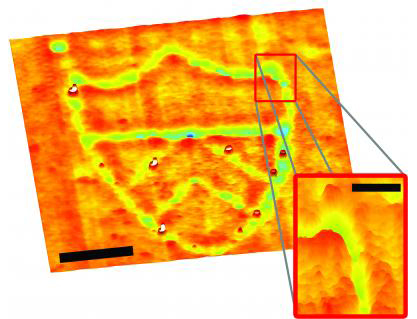
The researchers used the technique to “draw” features that were about 100 nanometers (a billionth of a centimeter) in size.
The key innovation is the use of a second, highly focused laser, which points directly down onto the bead. This intense light exerts a physical force on the bead, trapping it in the beam and pushing it down toward the surface. The surface pushes back with a constant force, and the bead settles at a height that balances the opposing forces. The original laser is then pulsed at the bead, which focuses the light to “zap” the surface directly below. By moving the bead along a computer controlled trajectory while repeating the laser pulse, a desired pattern is created.
The technique offers particular advantages on curved or irregular surfaces because the bead tracks the surface, moving up when there is a bump and dropping when it moves over a dip. While other fabrication techniques, such as electron-beam lithography, can also be used to pattern uneven surfaces, they are extremely expensive and must be performed in a vibration- and oxygen-free environment. The new Princeton technique can be performed in a regular environment, making it accessible for use with biological materials and other systems that require the presence of oxygen.
“The technique provides a very interesting new capability to expand laser-assisted nanofabrication without involving moving mechanical parts and related hardware complications,” said Costas Grigoropoulos, mechanical engineering professor at University of California-Berkeley. “I do expect that this novel technique will advance nanopatterning since it offers an elegant and highly effective means for parallel, optically driven and controlled nanofabrication.”
In addition to burning away parts of a chip, Arnold and McLeod’s method has the potential to deposit materials on surfaces, rather like gold-plating. This could provide a new means of creating three-dimensional structures, including miniscule guides that manipulate light and nanoscale electrical-mechanical devices. Such devices have many potential uses in ultrasmall sensor systems and low-power computer processors.
“In the future, we imagine the use of multiple beads of different shapes and sizes — in essence a nanopatterning toolkit — for researchers to pick and choose during the course of fabrication,” said Arnold. He and McLeod are currently working to pattern a surface using an array of many beads moving in parallel, each trapped and controlled by a different laser beam.
The research was supported by Princeton University and the Air Force Office of Scientific Research.


