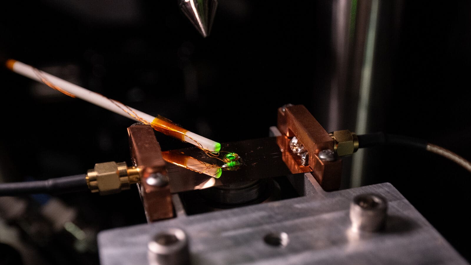
In pursuit of computers that harness the power of quantum mechanics, Andrew Houck carves sapphires into wafers thinner than a human hair and uses them to trap single particles of light. To do this, Houck must peer into the sapphire at the atomic level, a feat that he said requires “a shocking degree of precision.”
Houck, a professor of electrical engineering, performs much of the work at the Princeton Institute for the Science and Technology of Materials (PRISM). It is the kind of science and engineering made possible by recent upgrades to PRISM’s Imaging and Analysis Center (IAC) and Micro/Nano Fabrication Laboratory (MNFL).
“Having a central facility for characterizing and fabricating materials is absolutely critical for many areas of research,” said Craig Arnold, director of PRISM and a professor of mechanical and aerospace engineering. “It’s not just materials science – it’s energy, it’s environment, it’s health, it’s security.”
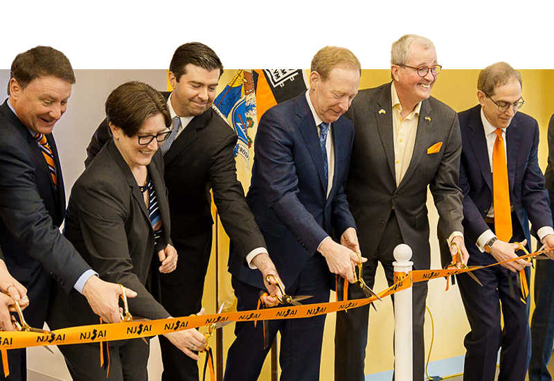
Speaking at a daylong event Oct. 26 to inaugurate the new facilities, Arnold said that major investments by the University have made the imaging center and fabrication lab among the best in the world and perhaps unique in their “one-stop-shop” combination of analysis and fabrication. The list of new equipment includes X-Ray tomography, atomic layer deposition, reactive-ion etching and a transmission electron microscope that is capable of viewing individual atoms and is one of only several in the world.
Open to researchers from outside of Princeton as well as from across the University, the facility is a prime example of “something Princeton does extraordinarily well, which is interdisciplinary research,” said Emily A. Carter, dean of the School of Engineering and Applied Science, as she welcomed participants. “Materials science and engineering is truly an enabling discipline for many applications that are so important for solving societal problems,” said Carter, who also is the Gerhard R. Andlinger Professor in Energy and the Environment and professor of mechanical and aerospace engineering and applied and computational mathematics.
The new tools will augment or provide upgrades to the approximately 100 pieces of equipment available at the shared-use facilities. (A full list of all the equipment is available at the IAC and MNFL websites.) Princeton researchers, along with external individuals, companies and institutions, can book time on the machines through online reservation systems.
At the inaugural event, Arnold and Carter emphasized that the power of the facilities comes from a combination of factors: the sophisticated building that houses them, the highly skilled research staff members who run them, and the equipment itself.
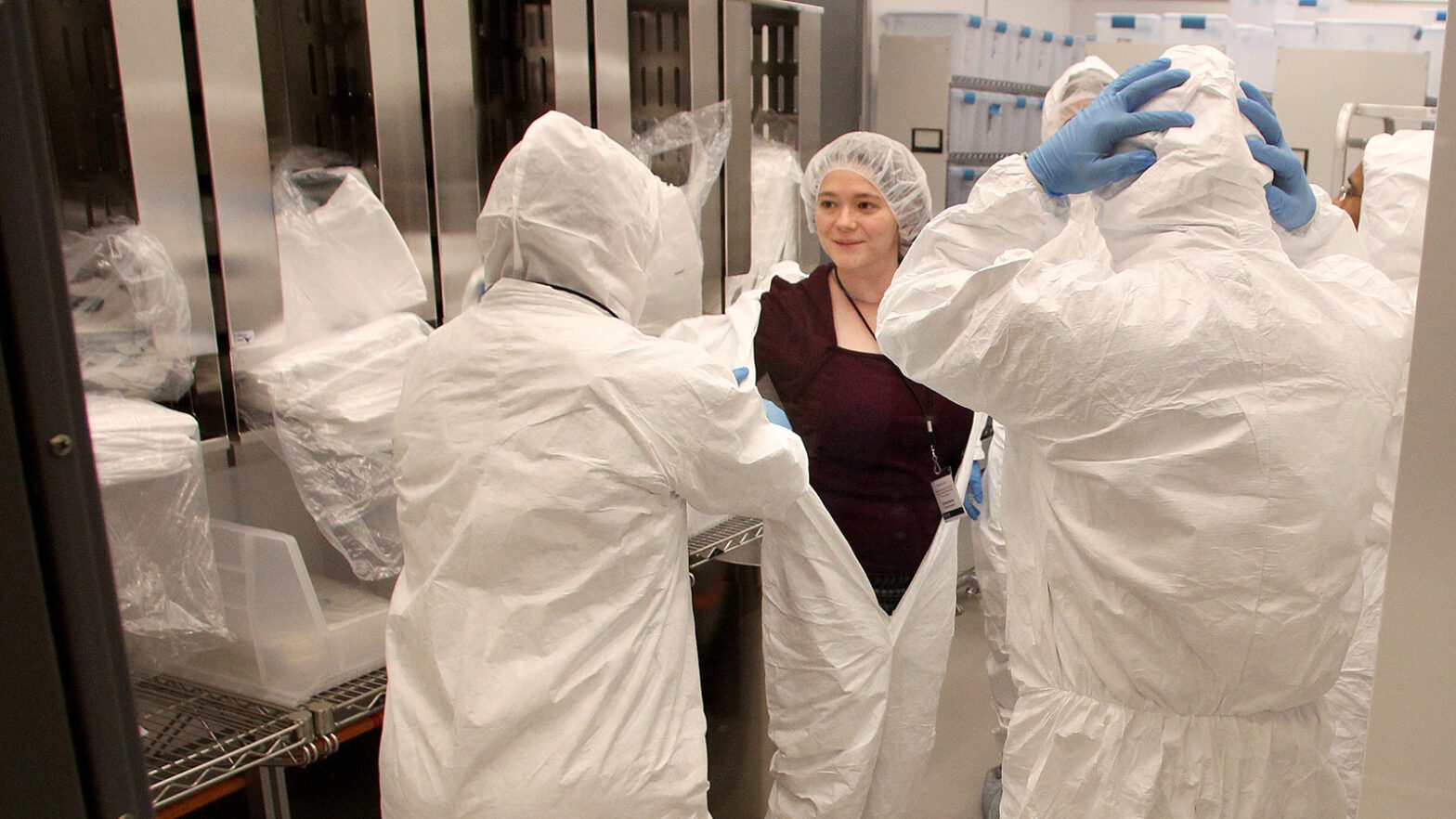
The imaging center and the fabrication lab moved this year from Bowen Hall to the newly constructed Andlinger Center for Energy and the Environment, which was designed expressly to optimize conditions for atomic-scale work. The new building is anchored in the underlying bedrock so that it is uncommonly free of vibration – it moves at 30 microinches per second as opposed to typical buildings that jiggle at about 16,000 microinches per second. To avoid electromagnetic interference, the entire analysis and fabrication area is encased in 100,000 pounds of 3/8 inch-thick aluminum. The fabrication area includes 27,000 square feet of “clean room” space that almost entirely eliminates dust particles that could interfere with nanometer-sized structures. Even the heating and cooling system introduces incoming air in smooth sheets that move evenly from ceiling to floor to avoid air currents that jostle the microscopes.

The inauguration-day presentations began in the Andlinger Center’s Maeder Hall Auditorium. In addition to talks by technical experts who discussed the capabilities of the equipment, speakers included Andrew Zwicker, head of outreach and education at the Princeton Plasma Physics Laboratory and member of the New Jersey General Assembly representing the 16th District, and Princeton alumnus Vladimir Buloviƒá, associate dean for innovation at the Massachusetts Institute of Technology.
In his talk, “The Future Will Be Measured in Nanometers,” Buloviƒá emphasized that key factors in biology and technology operate at the scale of nanometers (a billionth of a meter), which is the realm accessible in the Princeton facilities. The molecules that determine scents such as lemon or vanilla are slightly less than a nanometer in size, as are the features of materials that cause different colors, and the electronic properties that allow devices such as extremely lightweight solar cells.
“Right now we are charting the path forward like never before,” Buloviƒá said. “We are living in the renaissance era of nanotechnology.”
To work with these tiny materials, scientists must be able to “see” them, although they are often operating at scales far below objects that can be viewed with light. To do this, the University offers an array of instruments. One of the most exciting, the transmission electron microscope (TEM), operates by streaming a beam of electrons through a thin sample of material. The electrons interact with the sample’s atoms and generate signals that reveal the most intricate properties.
“There are only a handful of TEMs like this one in the entire world,” Arnold said. “With it, you’re able to see down to individual atoms in a material and capture never-before-seen details of its structure.”
The level of detail achievable at the imaging center is bearing out the theoretical work begun in the 1980s by F. Duncan Haldane, a Princeton Eugene Higgins Professor of Physics. Haldane won a share of the 2016 Nobel Prize in Physics for his research using a branch of mathematics known as topology to describe the behaviors of exotic states and shapes of matter that could someday form the backbone of quantum computers.
“The materials that were predicted by Haldane are now routinely characterized in our facilities,” Arnold said.

Houck’s group will use the new imagers at the center to precisely visualize the patterns of the chemical element niobium etched onto ultra-high-purity sapphire wafers. When cooled to millionths of a degree above absolute zero, niobium atoms begin to display quirky quantum-mechanical properties that, if maintained and manipulated, could be used to run computations in a full-fledged quantum computer.
“The instrument allows us to image, characterize and see what’s going on with the things we’ve built and, if they’re not working right, to diagnose the problem,” Houck said.
The quantum-computational systems Houck and his colleagues aim to develop are extremely delicate and vulnerable to the slightest of outside perturbances, such as temperature and energy fluctuations. To maximize performance, the architectures in Houck’s experiments must be accurate down to the atomic scale.
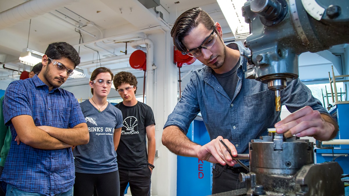
That precision is made possible by instrumentation at the fabrication lab. An example is a device called a DWL 66-fs Maskless Lithography Laser Writer made by the German company Heidelberg Instruments. The machine uses a laser to etch grooves and spaces into materials necessary for testing out quantum-computer component arrangements.
“The new lithography laser writer allows us to make patterns directly and quickly with more precision than ever had been available,” Houck said. “We are completely dependent on the MNFL. It’s the workhorse of our lab.”
Work pursued at the facilities also goes beyond quantum-computing research. It includes developing and understanding materials that could lead to improved batteries and organic light-emitting diodes, new sensors for environmental and health monitoring, and innovative microscopic machines.
“I recognize how fortunate we are at Princeton to have the resources that we do,” Arnold said. “We want the broader community to also benefit from the world-class facilities we have here on campus.”
———
Note: Please direct inquiries about using the facilities and collaborating with PRISM faculty to:
PRISM
Joseph Montemarano, jmonte@princeton.edu, 609-258-2267
Imaging and Analysis Center
Nan Yao, nyao@princeton.edu, 609-258-6394
Micro/Nano Fabrication Lab
Anthony Novembre, novembre@princeton.edu, 609-258-6855
